
12 years of hard work! Domestic germanium wafers and gallium arsenide wafers have made major breakthroughs.
Release time:
2021-06-05
Author:
Chip Master
Source:
Chip Master
Yesterday, Yunnan Daily released a piece of good news. After 12 years of hard work, core products such as "zero-position error" germanium wafers, indium phosphide wafers, and gallium arsenide wafers in Yunnan germanium industry have successfully broken through foreign technology blockades and monopolies.
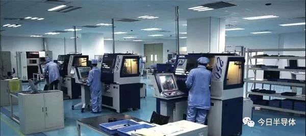
Production Line of Yunnan Germanium Industry
Introduction: On May 31, according to Yunnan Daily, after 12 years of tackling key problems, core products such as "zero error" germanium wafers, indium phosphide wafers and gallium arsenide wafers in Yunnan germanium industry have successfully broken through foreign technology blockades and monopolies.
According to the report, the above-mentioned products have been localized on the basis of mastering core key technologies and independent control. According to previous public reports, some products have been applied in batches to national defense projects and supporting domestic well-known chip manufacturers.
Yunnan germanium industry is the world's largest manufacturer and supplier of germanium series products and a leader in the new materials industry. The company has abundant germanium resources, the country's super-large germanium ore, germanium metal reserves of 890 tons, accounting for 26% of the country.
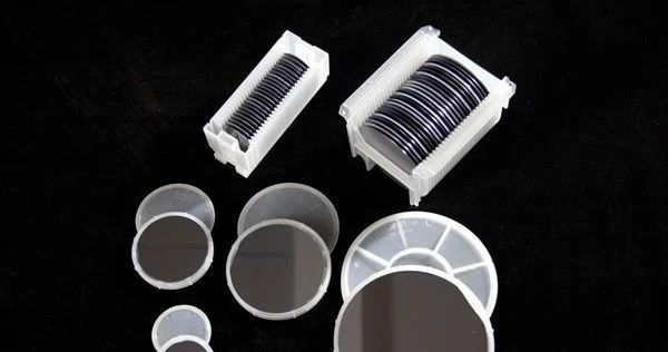
Figure: GaAs wafer
Among them, solar germanium wafers are widely used in space satellite solar cells, high-altitude unmanned reconnaissance aircraft, ground high-concentration solar power stations and other fields because of their high efficiency, high voltage and high temperature characteristics.
As the third generation semiconductor material, gallium arsenide has higher electron mobility and saturation migration speed than silicon. Semiconductor devices and semi-insulating devices made of gallium arsenide have high frequency, high temperature, low temperature performance, low noise, and strong radiation resistance.
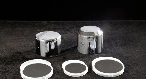
Indium Phosphide Wafer
The very characteristic compound semiconductor-indium phosphide wafer has a higher electron migration speed, suitable for the manufacture of high-speed, high-frequency low-power microwave, millimeter-wave devices and circuits, mainly used in the production of optical communication lasers and space detectors.
"Although these wafers have excellent physical properties, we have relied on imports for a long time and the preparation technology of wafers has been monopolized by foreign countries. To change this situation, we must break through the'zero mis' control technology." Huifeng, chief scientist of Yunnan germanium industry, introduced that during the production process of semiconductor single crystal, due to the fluctuation of external temperature and the influence of liquid surface convection, the atomic arrangement in the crystal cannot reach the ideal state, resulting in dislocation hyperplasia, crystal degeneration and product failure.
On the basis of establishing a cooperative relationship with the Chinese Academy of Sciences, Yunnan Germanium Industry has successively overcome key technologies such as temperature control, interface flatness and stability in the production process of semiconductor single crystal through continuous research and development, starting from the independent research and development of equipment. Solar germanium wafers, gallium arsenide wafers, indium phosphide wafers and other products have reached the world's advanced and domestic leading level of similar products. The products are also exported to Germany, South Korea and other countries.
"In order to meet the needs of high-tech at home and abroad, we will attack the large diameter of wafers, develop germanium wafers, gallium arsenide wafers and indium phosphide wafers to larger sizes, continue to tackle key problems in the direction of ultra-thin wafers and improve the qualification rate of wafers, continuously reduce costs, improve the degree of industrialization, and build an aircraft carrier cluster of optoelectronic semiconductor materials in China." Bao Wendong, chairman of Yunnan germanium industry, said.
Previous article
Previous article
Related News
Tender Letter of Guangdong Fenghua Core Electric Technology Co., Ltd.
Semiconductor wafer production capacity is in short supply, coupled with the tight automotive chips, resulting in the back-end sealing capacity burst. Semiconductor production capacity is in short supply, capacity plug explosion situation from wafer foundry extended to the packaging and testing industry, the original tight supply of packaging materials is not enough, delivery time and price increase, affecting the packaging and testing capacity, IC designers must ensure the packaging and testing capacity through price increases or signing long contracts.
Contact Us
Guangdong Fenghua Semiconductor Technology Co., Ltd.
-
Company Office Number:+86 020-82075328
-
E-mail:hanziyang@nationstar.com
Address: No.10, Nanxiang 2nd Road, Science City, Luogang District, Guangzhou
WeChat public account

Copyright©2023 Guangdong Fenghua Semiconductor Technology Co., Ltd. |
| By:www.300.cn
| Business License | SEO