
Advanced Packaging War Begins
Release time:
2021-06-05
Author:
Semiconductor Industry Watch
Source:
Semiconductor Industry Watch
In the past two days, advanced packaging technology has set off a new wave of craze in Taiwan. The focus companies are AMD and TSMC.
This week, AMD announced that it has developed 3D chiplet technology with TSMC and will mass produce the corresponding chips by the end of this year. AMD President and CEO Su Zifeng said that the packaging technology is breakthrough. It uses advanced hybrid bond technology to combine AMD's chiplet architecture with 3D stack, providing interconnection density more than 200 times higher than 2D chiplet and density 15 times higher than existing 3D packaging solutions. It is reported that the technology developed by AMD in cooperation with TSMC has lower power consumption than existing 3D solutions and is also the most flexible active-on-active silicon stack technology in the world.
At present, as the most outstanding representatives of the two major fields of Fabless and Foundry, the degree of attention of these two companies to advanced packaging technology also represents the general consensus of the industry.
Yole's data shows that in 2021, outsourced semiconductor packaging and testing (OSAT) companies will spend no less than $6.7 billion on advanced packaging technology research and development, equipment procurement and infrastructure construction. In addition, not only OSAT, TSMC and Intel also spend a lot on advanced packaging.
In this competition, the five most eye-catching companies are Sun Moonlight (ASE), TSMC, Intel, Amkor and Jiangsu Changdian (JCET). Among them, TSMC plans to spend US $2.5 billion to US $2.8 billion in 2021 to build packaging plants based on its product lines of INFO, CoWoS and SoIC. Yole estimates that TSMC generated $3.6 billion in revenue from advanced packaging in 2020.
In addition, OSAT overlord ASE announced that it will invest US $2 billion in its wafer-level packaging business. Intel announced that it will invest US $20 billion to build a fab in Arizona and expand its Foveros/EMIB packaging business in Arizona and Oregon factories. In addition, it will also invest in advanced packaging cooperation projects, mainly TSMC.
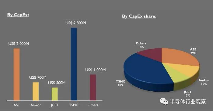
Figure: Projected capital expenditure for advanced packaging in 2021, source: Yole.
However, looking back over the past two years, the global advanced packaging market has experienced ups and downs.
In 2019, the advanced chip packaging market is worth about $29 billion out of a total $68 billion packaging market. At the time, market analysts said the advanced packaging market would grow at a compound annual growth rate (CAGR) of 6.6 percent between 2019 and 2025. The main driver of this market is the slowdown of Moore's Law, which has spawned heterogeneous integration. At the same time, applications including 5G, artificial intelligence, high-performance computing and Internet of Things are also driving the development of the advanced packaging market. In this context, by 2025, advanced packaging will account for about 50% of the total packaging market share.
However, after entering 2020, the sudden outbreak has had a greater impact on the semiconductor industry, the advanced packaging market industry was not immune, the year-on-year contraction, a decrease of 7%, while the traditional packaging market decreased by about 15%.
However, after entering 2021, the development of the semiconductor market has improved significantly, and the advanced packaging market has risen. In the coming second half of the year, the major manufacturers will further increase investment in this area in order to gain the first opportunity.
TSMC Leads in Advanced Packaging
This week, during the TSMC 2021 online technology seminar, in addition to introducing the planning and progress of advanced processes, the company also focused on the development of advanced processes, especially the disclosure of 3DFabric system integration solutions, and will continue to expand 3DFabric composed of 3D silicon stack and advanced packaging technology.
TSMC pointed out that for high-performance computing applications, a larger photomask size will be provided in 2021 to support integrated fan-out and package substrates (InFO_ OS) and CoWoSR packaging solutions, and use a wider range of layout planning to integrate "small chips" and high-bandwidth memory.
In addition, in terms of system integration chips, the version of chips stacked on wafers is expected to complete 7nm verification this year and start production in a new fully automated fab in 2022.
For mobile applications, TSMC introduced the InFO_ B solution, which integrates mobile processors into thin and compact packages, provides enhanced performance and power efficiency, and supports the dynamic random access memory stack required by mobile device chip manufacturers.
TSMC has also expanded its advanced packaging business to Japan, which also requires a significant investment. Japan's Ministry of Economic Affairs and Industry said that TSMC will set up a research and development base in Tsukuba, Ibaraki Prefecture, Japan, with a total funding of about 37 billion yen, and the Japanese government will contribute about 50% of the total funding to support it. It is reported that about 20 Japanese enterprises related to semiconductors, such as Ibiden, a Japanese enterprise with leading packaging technology, and Shipu Machinery (Shibaura Machine), a semiconductor device manufacturer, are expected to participate in research and development, with emphasis on "small chips" and 3D packaging technology.
In March this year, TSMC set up a subsidiary in Japan (TSMC Japan 3D IC Research and Development Center). In the future, TSMC plans to set up a production line for research in the clean room of a research institution (Industrial Technology Research Institute) related to the Ministry of economy, trade and industry in Tsukuba City, Ibaraki Prefecture. It is expected that the test production line will be prepared this summer and will be officially developed next year.
Intel Investment $3.5 billion
In May, Intel announced that it would invest $3.5 billion to equip its Rio Rancho plant in New Mexico with advanced packaging equipment, including Foveros technology. Construction is expected to start by the end of 2021.
Intel introduced the Advanced Packaging Technology Foveros in 2019, which allows die to achieve 3D "face-to-face" stacking. Allows the base unit die to have a more "active" die on top, such as logic, memory, FPGA or analog/RF die.
At present, in terms of advanced packaging technology and business model, Intel is moving closer to TSMC, which also reflects the success of TSMC's development strategy and investment in this field in recent years.
Not long ago, Intel released the IDM 2.0 strategy. The company said that a key point of the strategy is advanced packaging, which enables Intel to provide better products.
The sun and moon ushered in the "sweet spot"
Recently, it has been reported that Riyueguang has won orders for SiP (System-in-Package) modules such as Apple Watch, WiFi 6/6E and AirPods. Judging from the current market situation, SiP will continue to maintain a rapid development momentum in 2021.
Since 2020, Riyueguang has made a number of achievements in advanced packaging research and development, including: flip-chip packaging, 7nm/10nm chip process technology certification, 14nm/16nm copper process/ultra-low dielectric chip flip-chip packaging application, silver alloy wire in hybrid flip-chip grid array packaging technology; In terms of bonding wire packaging, developed the second generation of advanced integrated component embedded packaging technology, ultra-fine pitch and wire diameter copper/gold wire technology, mobile storage technology, wafer-level fan-out RDL wire packaging, there are fan-out 30um chip thickness cutting technology before grinding, 8 Hi HBM CPD wafer high precision (/-2um) grinding technology, wafer through vias, glass substrate packaging, wafer-level chip size six-sided protection packaging technology development, fan-out PoP chip product development, and die bonding wafer process technology. In terms of advanced packaging and modules, developed low-power antenna design and packaging technology, flexible substrate and packaging technology, double-sided thinned wireless communication module technology, 5G antenna packaging, etc., panel-level packaging, the development of fan-out dynamic compensation mask panel-level packaging technology.
On this basis, Sun Moonlight will continue to expand the scale of advanced processes and production capacity in 2021, especially in 5G, SiP, sensors, automotive electronics and intelligent devices, and will further increase investment. In addition, it is expected that the demand for multi chips and sensors will increase, which will become the "sweet spot" of the company's production ".
Amkor's strength is not bad.
Amkor is also a force in advanced packaging technology, with customers in multiple markets using Amkor's advanced technology to achieve miniaturization, improve performance and reliability, and reduce system costs. These increased demand for advanced packaging, particularly advanced SiP packaging, drove the company's revenue growth. Amkor's SiP package has established itself in the consumer and automotive markets, and has also shown strength in the smartphone market.
Jiangsu Changdian counterattack
In the past year, Jiangsu Changdian Technology has continuously increased its R & D investment, and R & D expenses have increased by 5.2 year-on-year. The core technology covers various advanced packaging technologies, and will achieve a substantial increase in advanced packaging revenue in 2020.
Specifically, in terms of SiP, especially in the field of RF SiP packaging, Changdian Technology continues to accumulate advantages, to undertake 5G applications and other communications market packaging needs have played a decisive role. At the end of 2020, 5 billion the approval of the targeted issuance, the production capacity and technical advantages of Changdian Technology in this field will continue to expand.
In wafer-level packaging, the technology leadership of Changdian Technology is also expanding. Considering portability, customers in the consumer electronics market tend to have strict chip package size requirements, such as TWS headphones and other popular products must use wafer-level packaging technology to meet the size requirements. Changdian Technology is already the largest supplier of eWLB and WLCSP packaging, and demand for wafer-level packaging products will continue to grow as consumer electronics head customers continue to integrate and concentrate.
Recently, Changdian Technology also established the "Automotive Electronics Center". Automotive chips have high reliability requirements, and capacity certification in line with vehicle regulations requires long-term investment and planning. Changdian Technology not only has the traditional packaging of the car gauge production capacity, and in the car gauge products continue to innovate, car gauge-level flip-chip products are moving towards large-scale mass production.
Conclusion
As the chip process node continues to shrink, Moore's law is approaching the limit, advanced packaging is the inevitable choice of the post Moore era. Among them, SiP is one of the important development directions of semiconductor packaging, which has the advantages of short research and development cycle and space saving, and is the focus of the long-term strategic layout of leading packaging enterprises.
In addition, packaging is becoming more and more important to improve the overall performance of the chip. As advanced packaging develops in the direction of miniaturization and integration, technical barriers continue to increase. In the future, the scale of the advanced packaging market is expected to increase rapidly, and leading technology manufacturers will enjoy the largest dividends.
Related News
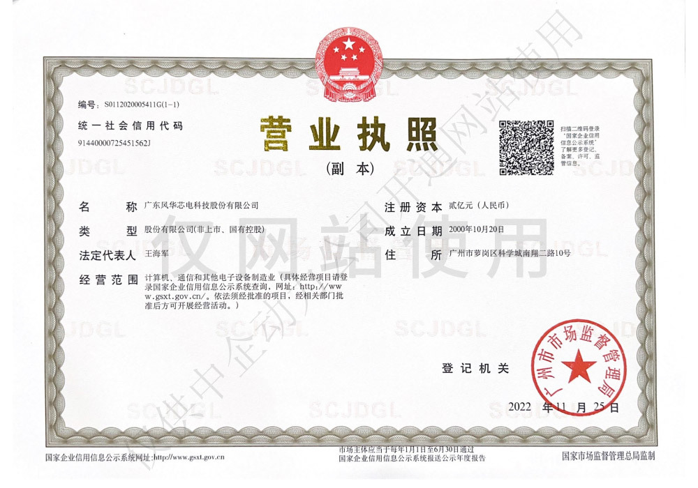
Tender Letter of Guangdong Fenghua Core Electric Technology Co., Ltd.
Semiconductor wafer production capacity is in short supply, coupled with the tight automotive chips, resulting in the back-end sealing capacity burst. Semiconductor production capacity is in short supply, capacity plug explosion situation from wafer foundry extended to the packaging and testing industry, the original tight supply of packaging materials is not enough, delivery time and price increase, affecting the packaging and testing capacity, IC designers must ensure the packaging and testing capacity through price increases or signing long contracts.
Contact Us
Guangdong Fenghua Semiconductor Technology Co., Ltd.
-
Company Office Number:+86 020-82075328
-
E-mail:hanziyang@nationstar.com
Address: No.10, Nanxiang 2nd Road, Science City, Luogang District, Guangzhou
WeChat public account

Copyright©2023 Guangdong Fenghua Semiconductor Technology Co., Ltd. |
| By:www.300.cn
| Business License | SEO